Introduction to Head-In-Pillow
1. Head-In-Pillow: There is no complete wetting between the solder ball and the solder paste during the reflow stage.
2. The manifestation of the ball and socket defect is that the solder ball seems to be connected to the entire solder paste, but in fact it is only placed in a pit or pile that does not form a mutual fusion.
3. Ball and socket defects can sometimes cause after-sales failures and reliability failures through functional tests, so they are extremely harmful.
I.C.T is a manufacturer of SMT machines. It mainly provides customers with SMT production lines including SMT Stencil Printers, Pick and place machines, Reflow Oven, AOI Machine, Wave Soldering Machine and PCB Handling Machine etc. I.C.T has more than 25 researches on SMT and DIP technology, for the world Customers provide SMT total solutions. There are successful cases of SMT technICal team in Asia, Europe, AmerICa, AfrICa, and Australia.
More details, please contact us:
Tel: +86 13670124230 (WhatsApp/Skype/WeChat)
Email: etaSMT@foxmail.com
The formation mechanism of Head-In-Pillow
Potential causes of head-in-pillow (Head-In-Pillow)
Different Views on Solving Head-In-Pillow
+ Extend the temperature of the holding area to reduce the temperature difference
+ Steel mesh reaming 2~4mils
+ Use solder paste that resists ball and socket defects
+ Increase the stencil opening of the corner pad of the component
+ Reduce reflux holding time
+ Use nitrogen reflux
+ Improve solder paste composition to increase thermal resistance, accelerate wetting time and maintain good wetting stability
Defect description and production information (actual case)
Picture Defect Analysis-Steel Mesh Design
+ Screen design-The stencil design in the table (1) meets the stencil design standard, and the solder paste printing volume is sufficient.
Defect Analysis-Solder Paste Printing
+ Solder Paste Printing-The results of red ink dyeing experiment and slicing experiment show that the amount of solder paste is sufficient
Defect analysis-placement accuracy
Placement accuracy-The slicing result at the defect location also tells us that there is no problem with placement accuracy.
Defect analysis-(thermal deformation) printed circuit boards and components
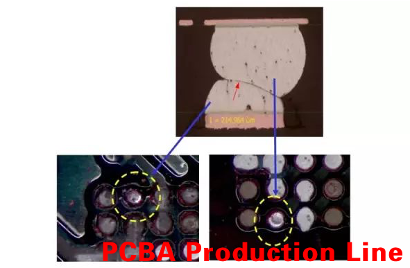
Thermal deformation of printed circuit boards & components-In some samples with serious defects, there is a clear gap between the BGA and the PCB, as shown in the figure below. Therefore, BGA packaging or PCB board warpage is an important point of suspicion.
HIP detection method: non-destructive inspection
Process optimization
Process optimization is mainly concentrated in two aspects
Process optimization-experiment
Summary & Conclusion
+ BGA/CSP packaging and PCB substrate warpage and excessive flux consumption can easily lead to ball sockets
The occurrence of defects.
+ Optimize the reflow soldering curve, by reducing the maximum temperature and shortening the time of the heating section from 190℃ to 220℃
Time can reduce the occurrence of ball and socket defects.
+ The use of solder paste with high temperature resistance and strong anti-oxidation protection flux can reduce the occurrence of ball and socket defects.
+ Under specific parameter settings and with a certain tilt angle, X-ray equipment can effectively capture ball and socket defects.
LED Lamp Machine Assembly Line, LED Bulb Assembly Machine Line, SMT Automatic Printer, Kik Reflow Oven Profiler, Acrab 450 Wave Soldering Machine, SMT Fuji Machine, Pick And Place SMT, SMD Pick And Place Machine Fully Automatic, Panasonic SMT Machin, SMT Machine Low Production, Desktop Pick And Place, Micro Robot Pick And Place, , PCBA Cleaning Machine, PCB Cleaning Machine, PCB Cleaner, Stencil Cleaning Machine, Stencil Cleaner, Machine Clean LED PCB, Robotic Arm Screw, Inline Screw Robot, Desktop Robotic Screw Fastening, Auto Fastening Auto-Screwdriving Machine Automatic Fixing Screw Robot