
Features of BGA package
From: Author: Publish time:2021-09-09 10:56 Clicks:0
BGA (Ball Grid Array) package, that is, the pin arrangement of the components is a ball grid array package. It is an array of solder balls made on the bottom of the package body substrate as the I/O end of the circuit and the printed circuit board (PCB) interconnection Pin. Compared with traditional foot-mounted devices (Leaded Divce such as QFP, PLCC, etc.), BGA packaged devices have the following characteristics.
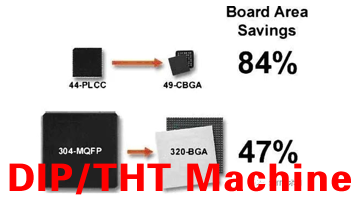
1) There are many I/Os: Generally, with the same number of leads, the package size can be reduced by more than 30%. For example: CBGA-49, BGA-320 (pin pitch 1.27 mm) compared with PLCC-44 (pin pitch 1.27 mm) and MQFP-304 (pitch 0.8 mm), the package size is reduced respectively 84% and 47%, as shown in the figure.
I.C.T is a manufacturer of SMT machines. It mainly provides customers with SMT production lines including SMT Stencil Printers, Pick and place machines, Reflow Oven, AOI Machine, Wave Soldering Machine and PCB Handling Machine etc. I.C.T has more than 25 researches on SMT and DIP technology, for the world Customers provide SMT total solutions. There are successful cases of SMT technICal team in Asia, Europe, AmerICa, AfrICa, and Australia.
More details, please contact us:
Tel: +86 13670124230 (WhatsApp/Skype/WeChat)
Email: etaSMT@foxmail.com
2) Improve the placement yield and potentially reduce costs.
3) The contact surface between the BGA array solder balls and the substrate is large and short, which is good for heat dissipation.
4) The BGA array solder ball pins are very short, which shortens the signal transmission path and reduces the lead inductance and resistance, thus improving the performance of the circuit.
5) The coplanarity of the I/O end is obviously improved, and the loss caused by the poor coplanarity during the assembly process is greatly reduced.
6) BGA is suitable for MCM packaging and can realize the high density and high performance of MCM.
7) Both BGA and CBGA are stronger and more reliable than ICs with fine pitch footprint packages.
2 Structure type of BGA package
There are many types of BGA packages, and the outline structure is square or rectangular. According to the arrangement of its solder balls, it can be divided into peripheral type, staggered type and full array type BGA. According to the different substrates, it is mainly divided into three categories: PBGA (Plastic Ball Grid Array), CBGA (Ceramic Ball Grid Array), and TBGA (TapeBall Grid Array).
Through the analysis and comparison of the characteristics and structure of BGA packages, the advantages and disadvantages of BGA devices are as follows:
1) Advantages: small size, light weight, strong function.
2) Disadvantages: high sensitivity to humidity, fragile structure, poor fatigue resistance of solder joints, poor shear stress of solder joints, and reduced reliability.
Schematic diagram of mainstream BGA package structure at this stage
With the increasing number of packaged devices such as Flip-Chip and BGA, the number of spherical pins of this type of device has increased, forcing the size of the solder joints for circuit interconnection to shrink, although the size of the electronic products we produce is getting smaller and smaller, The weight is getting lighter and lighter, but the connection strength between the device and the printed circuit board and the insulation between the pins are becoming more and more fragile. Therefore, potting or filling the bottom of the BGA packaged device with glue is necessary for the long-term reliability of flip-chip assembly. The potting or filling at the bottom of the device can reduce the stress of the solder joints, evenly disperse the stress on the packaging surface of the flip chip, and at the same time can increase the mechanical and electrical insulation strength of the device.
Therefore, the bottom of the soldered BGA device is filled with glue to reduce the sensitivity of the BGA device to humidity, enhance the structure of the BGA device, improve the fatigue resistance of the solder joint, improve the shear stress of the solder joint, and improve the reliability of the product. Craftsmanship is a very necessary and necessary work.
Therefore, the selection of bottom potting materials is also a very important task. For CSP and BGA bottom potting materials, it should be easy to use, store and transport, and should meet the required reliability requirements. For the production process, such as: the storage conditions of the glue, the service life, the potting properties, the flow speed of the glue at the bottom of the chip, and the curing time are all parameters that should be considered. If the value of the circuit board is high, the repairable bottom potting material should be used. Therefore, in this case, the easy repairability of the chip after potting is particularly important; in terms of the reliability of the potting, there is no bubble or drop Life test and thermal shock life test are several important factors for electronic equipment. Automobiles and military electronic products have more stringent requirements for resistance to shock, shock resistance, and severe thermal shock. This article focuses on the analysis of CSP/BGA bottom potting material selection and the realization of the operable process.
3 Bottom potting material
Most bottom potting adhesives are one-component thermal curing epoxy adhesives. It can be cured quickly, with high bonding performance, low modulus and strong repairability. Good temperature resistance and good storage stability.
3.1 The main components and functions of epoxy resin potting compound
The role of epoxy resin potting compound is to strengthen the integrity of electronic devices, improve resistance to external shocks and vibrations; improve the insulation between internal components and circuits, which is conducive to miniaturization and light weight of devices; avoid direct exposure of components and circuits, Improve the waterproof and moisture-proof performance of the device.
One-component epoxy resin potting compound is a multi-component composite system, which is composed of resin, curing agent, toughening agent, filler, etc., for the viscosity, reactivity, service life, heat release, etc. of the system It is necessary to make a comprehensive design in terms of sub-formulation, process, casting size structure, etc., to achieve a comprehensive balance.
There are many types of potting and sealing materials currently in use, such as DU901, DU902, DU986, DU902N made in Korea, 3513 and other models of American products Loctite (manufactured in Yantai, Shandong), and some products of Debon (manufactured in Yantai, Shandong). And some of the three arrows of JIAPAN, CSP/BGA bottom potting glue 3113 produced by Sumitomo and Beijing United Titan, etc. But at present, the most used one should still be Loctite's 3513.
During the experiment, we chose CSP/BGA bottom potting glue 3513 produced by LOCTITE Company for experiment. The following table is the performance table of this material.
LED Bulb Assembly Line Machine, LED Lamp Line Assemble, Solder Paste Screen Printer, Solder Paste Printer Line, Reflow Oven 2520, Oven Reflow, Wave Soldering Machine Desktop DIP China, Laser Coding Machine SMT Assembly Inline, SMT YSM20R Pick And Place Machine, SMT Component Carrier Tape Packaging Machine, SMT Pick And Place Machine Benchtop, SMT Drill Machine Price In Pakistan, Automatic SMT Selective Coating Machine, PCB Belt Conveyor, PCB Assembly Conveyor Table, PCB Flipper Inverter Conveyor, SMT Screening Conveyor PCB, SMT Screening Conveyor, Laser PCB Separator, Aurotek PCB Separator