
Types and design standards of pads in PCB design
From: Author:Mark Hardy Publish time:2021-09-09 13:54 Clicks:0
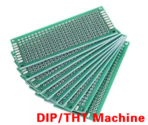
Let’s learn about the types of pads and the design standards of pads in PCB design today. The land, the basic unit of surface mount assembly, is used to form the land pattern of the circuit board, that is, a variety of land combinations designed for special component types.
I.C.T is a manufacturer of SMT machines. It mainly provides customers with SMT production lines including SMT Stencil Printers, Pick and place machines, Reflow Oven, AOI Machine, Wave Soldering Machine and PCB Handling Machine etc.
More details, please contact us:
Tel: +86 13670124230 (WhatsApp/Skype/WeChat)
Email: etaSMT@foxmail.com
The pad is used for electrical connection, device fixing, or part of the conductive pattern that combines both.
Types of PCB pads
One, common pad
1. Square pad
It is often used when the components on the printed circuit board are large and few, and the printed wires are simple. It is easy to use this kind of pads when making a PCB by hand.
2. Round pad
It is widely used in single and double-sided printed boards with regularly arranged components. If the density of the board allows, the pad can be larger so that it will not fall off during soldering.
3. Island pad
The connection between the pad and the pad is integrated. It is often used in vertical irregular arrangement installation.
4. Polygonal pad
Used to distinguish pads with close outer diameters but different apertures, which is convenient for processing and assembly.
5. Oval pad
This kind of pad has enough area to enhance the anti-stripping ability, and is often used in dual in-line devices.
6. Open-shaped pad
In order to ensure that after wave soldering, it is often used when the manually repaired land hole is not sealed by solder.
Two, special pads
1. Plum blossom pad
Torx pads are usually used in large vias to ground. There are several reasons for this design:
1) The fixing hole needs to be metallized and connected to GND. If the fixing hole is fully metallized, it is easy to block the hole during reflow soldering.
2) The use of internal metal screw holes may cause the grounding to be in a bad state due to installation or multiple disassembly and assembly. However, the use of quincunx pads can ensure a good grounding regardless of the change in the stress.
2. Cross flower pad
Cross flower pads are also called thermal pads, hot air pads, and so on. Its function is to reduce the heat dissipation of the pad during soldering, so as to prevent false soldering or PCB peeling caused by excessive heat dissipation.
1) When your pad is ground. The cross pattern can reduce the area of the ground wire, slow down the heat dissipation speed, and facilitate welding.
2) When your PCB requires machine placement, and it is a reflow soldering machine, the cross-pattern pad can prevent the PCB from peeling (because more heat is needed to melt the solder paste).
It is often used when the traces connected to the pads are thin to prevent the pads from peeling and the traces are disconnected from the pads. Such pads are commonly used in high-frequency circuits.
Design standards for pads in PCB design
1. The shape and size design standard of PCB pad
1. The minimum single side of all pads is not less than 0.25mm, and the maximum diameter of the entire pad is not more than 3 times the component aperture.
2. Try to ensure that the distance between the edges of the two pads is greater than 0.4mm.
3. In the case of dense wiring, it is recommended to use oval and oblong connecting plates. The diameter or minimum width of the single-sided board pad is 1.6mm; the weak-current circuit pad of the double-sided board only needs to add 0.5mm to the hole diameter. Too large the pad will easily cause unnecessary continuous soldering. The diameter of the hole exceeds 1.2mm or the diameter of the pad. The pads over 3.0mm should be designed as diamond or quincunx pads.
4. For plug-in components, in order to avoid the phenomenon of copper foil breaking during welding, and the single-sided connecting plate should be completely covered with copper foil; the minimum requirement for double-sided panels should be filled with teardrops.
5. All machine insert parts need to be designed as drip pads along the bent leg direction to ensure full solder joints at the bent leg.
6. The pads on the large-area copper skin should be chrysanthemum-shaped pads, which should not be soldered. If there is a large area of ground and power lines on the PCB (with an area of more than 500 square millimeters), the window should be partially opened or designed to fill the grid.
LED Screen Assembly Line, LED Lamp Assembly Line, Printing Stencils, Screen Printing Stencils, LED Special Vacuum Reflow Oven, Batch Benchtop Nitrogen Reflow Oven, Wave Soldering Machine, Laser Coding Machine SMT Assembly, Juki SMT Machine Spare Parts, SMT Light Testing Machine LED, Empty Reel For SMT Machine, SMT PCB Suction Board Machine, SMT Machine For Bar Phones, PCB Chain Conveyor, 1.5M PCB Conveyor, PCB Inspection Conveyor, PCB Stack Conveyor, PCB Assembly Conveyor, Depaneling Machine V-Cut PCB Separator, Soldering Robot, Cheap Soldering Robot, Automatic Soldering Robot, Soldering Robot Automatic