
Component failure analysis method
From: Author:Mark Hardy Publish time:2021-09-09 15:14 Clicks:0
Once the device is broken, don't stay away from it, but should be like a treasure.
Everyone who drives knows, where is the best way to practice driving? Highways are not good, only busy cities and bad road conditions can improve the level. The development of society is a process of discovering and solving problems. It is not terrible to have problems, but it is very terrible to have the same type of problems frequently.
I.C.T is a manufacturer of SMT machines. It mainly provides customers with SMT production lines including SMT Stencil Printers, Pick and place machines, Reflow Oven, AOI Machine, Wave Soldering Machine and PCB Handling Machine etc. I.C.T has more than 25 researches on SMT and DIP technology, for the world Customers provide SMT total solutions. There are successful cases of SMT technICal team in Asia, Europe, AmerICa, AfrICa, and Australia.
More details, please contact us:
Tel: +86 13670124230 (WhatsApp/Skype/WeChat)
Email: etaSMT@foxmail.com
Basic concepts of failure analysis
Definition: The process of diagnosing failed electronic components.
1. Failure analysis often requires electrical measurement and the use of advanced physical, metallurgical and chemical analysis methods.
2. The purpose of failure analysis is to determine the failure mode and failure mechanism, and propose corrective measures to prevent the recurrence of this failure mode and failure mechanism.
3. Failure mode refers to the observed failure phenomenon and failure form, such as open circuit, short circuit, parameter drift, functional failure, etc.
4. Failure mechanism refers to the physical and chemical process of failure, such as fatigue, corrosion and overstress.
General procedure for failure analysis
1. Collect field data
2. Electrical measurement and determination of failure mode
3. Non-destructive inspection
4. Open the package
5. Mirror
6. Power on and locate the failure
7. Perform physical and chemical analysis on the failure location to determine the failure mechanism.
8. Comprehensive analysis, determine the cause of failure, and propose corrective measures.
1. Collect field data:
Type of stress
experiment method
Possible main failure modes
Electrical stress
Static electricity, excessive electricity, noise
Gate breakdown of MOS devices, pn junction breakdown of bipolar devices, secondary breakdown of power transistors, latch-up effect of CMOS circuits
Thermal Stress
High temperature storage
Al-Si in metal-semiconductor contact is mutually soluble, ohmic contact is degraded, pn junction leakage, Au-Al bonding failure
Low temperature stress
Low temperature storage
Chip break
Low temperature electrical stress
Low temperature work
Hot carrier injection
High and low temperature stress
High and low temperature cycle
Chip breakage, chip bonding failure
Thermoelectric stress
High temperature work
Metal electromigration, ohmic contact degradation
Mechanical stress
Vibration, shock, acceleration
Chip breakage, lead breakage
Radiation stress
X-ray radiation, neutron radiation
Electrical parameter changes, soft errors, latch-up effects of CMOS circuits
Climatic stress
High humidity, salt spray
Outer lead corrosion, metallization corrosion, electrical parameter drift
2. Electrical measurement and determination of failure mode
Electrical measurement failures can be divided into connectivity failures, electrical parameter failures and functional failures.
Connectivity failures include open circuits, short circuits, and resistance changes. This type of failure is easy to test, and most of the field failures are caused by electrostatic discharge (ESD) and electrical stress (EOS).
The electrical parameters are invalid, and more complicated measurements are required. The main manifestations are that the parameter value exceeds the specified range (out of tolerance) and the parameter is unstable.
To confirm that the function is invalid, input a known excitation signal to the component and measure the output result. If the measured output state is the same as the predicted state, the component function is normal, otherwise it is invalid. The function test is mainly used for integrated circuits.
The three types of failures have a certain correlation, that is, one type of failure may cause other types of failures. The root cause of functional failure and electrical parameter failure can often be attributed to connectivity failure. In the absence of complex functional testing equipment and testing procedures, it is possible to use simple connectivity testing and parameter testing methods for electrical testing, combined with the application of physical failure analysis techniques to still obtain satisfactory failure analysis results.
3. Non-destructive inspection
name
Application advantage
Main principle
X-ray fluoroscopy
With the low-density area as the background, observe the density anomalies in the high-density area of the material
The abnormality of X-ray imaging after being partially absorbed by the sample
Reflection scanning acoustic microscopy (C-SAM)
Take the high-density area as the background to observe the voids or low-density areas inside the material
Ultrasonic wave is hindered and reflected by the gap
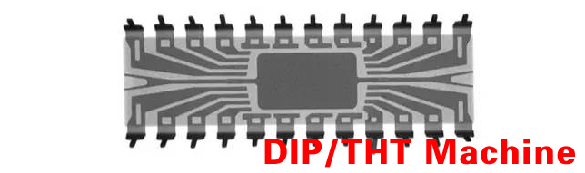
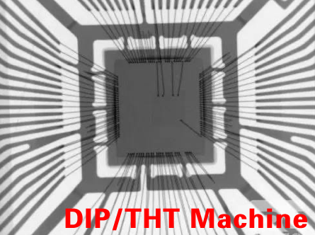
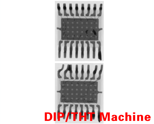
X-Ray inspection is to use X-ray to see through components (multiple directions and angles are optional) without destroying the chip, to detect the packaging of components, such as bubbles, abnormal bonding wires, die size, and bracket direction Wait.
picture
Applicable scenarios: check whether there is any abnormality in the bonding, whether the package is defective, confirm the die size and layout
Advantages: short construction period, intuitive and easy to analyze
Disadvantage: limited access to information
Limitations:
1. The internal shapes of the devices of the same batch of devices in different packaging production lines are slightly different;
2. The internal circuit damage or defect is difficult to detect, and it must be obtained through functional tests and other tests.
LCD TV Assembly Line, SMT Flexible LED Production Line, Printer PCB SMT Stencil Printer, Precision Stencil Printer SMT Machine, Bench Top Reflow Oven, Solder Machines, Pick And Place Nozzle, Sm471 Pick And Place, Intelligent Pick And Place, Pick And Place Unit, Pick And Place Amchine, Pick And Place Head Assembly, Pick And Place Machine Small, Simens Pick And Place Machine, PCB Loader Equipment, Cheap PCB Loader, PCB Handling Equipment Loader, SMT PCB Mini Loader, Cheap PCB Loader Machine, 5-Axis Desktop Soldering Robot, Automatic LED Spot Soldering Robot Machine