3 Steel mesh
The stencil is the SMT template, which is a special SMT mold. Its main function is to help the deposition of solder paste. The purpose is to transfer the exact amount of solder paste to the exact position on the empty PCB. It is the basic tool of the printing process. Its material Mainly 304 stainless steel sheet and FG steel sheet, which are the key tooling for printing solder paste. The thickness of the stencil and the size of the opening, the shape of the opening, and the state of the inner wall of the opening determine the amount of solder paste printed, so the quality of the stencil directly affects the amount of solder paste printed.
3.1 Processing technology of steel mesh
The current production methods of steel mesh mainly include laser cutting, chemical etching and electroforming. The production method and characteristics of Sanzhong steel mesh are shown in the following table:
picture
With the development of electronic products towards miniaturization and high functionality, in order to adapt to the application of high-density micro-pitch components and meet the printing of fine-pitch components, the traditional laser cutting stencil has been technologically innovated, and FG stencils and nano-coatings have appeared. New steel mesh production methods such as steel mesh.
FG steel mesh: a laser steel mesh made of special stainless steel fine-grained stainless steel. Its advantage is that a niobium element is added to the steel sheet production process. The niobium element can refine the grain, reduce the overheating sensitivity of the steel and increase the fire brittleness of the steel. Sheet processing strength; hole wall smoothness processing deformation variables are better than ordinary steel mesh, compared with ordinary 304 stainless steel, fine-grained stainless steel has the advantages of high tensile strength, good flexibility, and wear resistance. The laser template produced in this way has stable and consistent performance, excellent demolding performance, durability, and can effectively improve the one-time pass rate of printing.
More details, please contact us:
Tel: +86 13670124230 (
WhatsApp/Skype/WeChat)
Nano steel mesh: Nano steel mesh inherits the advantages of laser steel mesh with high precision and short processing time. Nano materials are combined with the surface of the contact surface of the PCB board and the inner wall of the mesh through nanotechnology, and the nano material structure is changed to make it With a good combination of stainless steel, the hardness of the steel will be greatly improved. Because nanomaterials have a repellent effect on the flux in the solder paste, it reduces the adhesion of the solder paste and the soldering flux, reduces the residue of the solder paste on the hole wall, and improves the demolding quality and the solder paste transfer rate.
3.2 Steel mesh design
Steel mesh design is the core of process design. Steel mesh design includes opening design and thickness design.
Thickness design: The thickness of the steel mesh should be determined according to the printed board assembly density, the size of the components, and the spacing between the pins (or solder balls). Generally, steel sheets with a thickness of 0.1 mm~0.13 mm are used. For high-density assembly, the thickness of 0.1 mm or less can be selected. 0.4 PITCH QFP, 0201 components, the appropriate thickness is 0.1 mm, 0.4 PITCH CSP components, the appropriate thickness is 0.08 mm.
Opening design: Including opening size and opening shape, both opening size and opening shape will affect the filling and release (release) of solder paste, and ultimately affect the printing volume of solder paste. The three major factors affecting the release of solder paste are: width-to-thickness ratio and area ratio; hole wall geometry; hole wall roughness.
The most basic requirements for stencil opening design: IPC-7525 defines the basic definition of stencil openings. It requires that the opening of the stencil must meet a certain aspect ratio and area ratio before the solder paste can be smoothly transferred to the PCB through the mesh. Its definition design The area ratio and width-to-thickness ratio of the stencil opening are respectively greater than 0.66 and 1.5, but in the actual design, the minimum width of the opening should be considered> 5*solder ball size, and the transfer rate of the solder paste that meets the above requirements will be more than 70%. When designing the steel mesh, if L>5 W, consider the aspect ratio; otherwise, consider the area ratio to measure whether the mesh design is conducive to the release of solder paste.
Aspect Ratio = Opening width (W)/Template thickness (T). Aspect ratio: W/T>1.5
Area Ratio=Area of opening/Area of hole wall. Area ratio: L×W/2(L+W)×T>0.66
picture
The stencil opening is designed according to the printed board land pattern, and sometimes needs to be appropriately modified (enlarge, reduce or modify the shape) because the structure, shape, and size of the different component pins require different amounts of solder paste. The stencil design must take into account the needs of different components on the board: the correct amount of solder paste required to form a reliable solder joint; good shape after release, reliable device contact and stability; good substrate interface, no solder balls, short circuits, etc. , Reduce the frequency of cleaning; easy to locate and print, with good process control ability. Several types of device opening methods are listed below, and the examples are all batch verification OK.
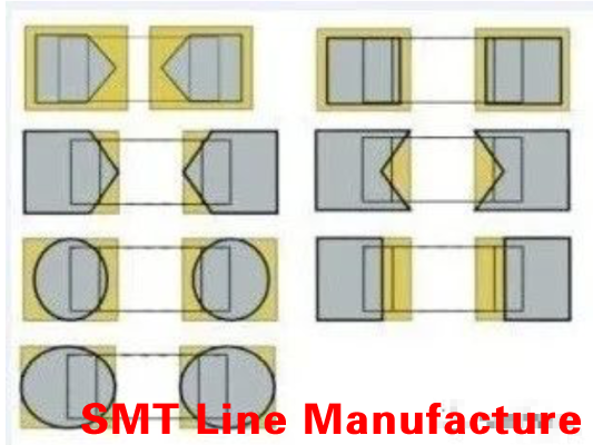
Chip component anti-solder bead opening: the generation of solder bead is due to the solder paste being squeezed out of the pad when the component is mounted. The solder mask on the surface of the component body and the printed board is incompatible with the solder paste and cannot produce wetting After the solder paste is melted, under the weight of the component body, the solder paste cannot rely on its surface tension to gather back to the pad, and part of it remains at the bottom of the component. When the component cools and solidifies, the remaining molten tin is squeezed out by the component sinking. , Form tin beads on the non-soldering position on the side of the component. Since the solder ball is caused by the tin overflow pad at the bottom of the component, it is necessary to consider reducing the amount of solder paste at the bottom of the component when designing the stencil, and minimize the contact and extrusion of the component body (non-soldering position) with the solder paste. For the resistance, capacitance, inductance, etc., pay attention to the matching of the internal distance of the opening and the components. The common opening designs are as follows:
Here is an example of optimizing the stencil opening design to solve the problem of tin bead caused by the mismatch between the inner distance of the diode pad and the components. (Steel mesh thickness T=0.12 mm)
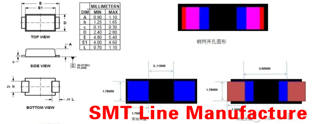
Fine-pitch BGA components prevent small tin openings: With the widespread use of fine-pitch BGA components, the requirements for stencil design are getting higher and higher. It is necessary to consider the thickness of the stencil and the selection of the production process, as well as the opening design to prevent The short circuit should also prevent the problem of less tin. For fine-pitch BGA components, it is usually necessary to ensure that there is enough gap between the meshes to prevent short circuits. However, if the amount of solder paste is too small, the volume of the solder joints will decrease, and reliability problems will ensue. For such packaged components, square openings and rounded corners are generally considered, which can increase the volume of the printed solder paste and improve reliability. The white part in the figure below is the shape and size of the PCB pad, and the red part is the shape of the stencil opening. Rounding is generally performed around the opening. The diameter of the rounded corner must be at least larger than the diameter of the tin powder to prevent the tin powder from blocking the corners during the printing process and causing the problem of less tin.
picture
0.8 mm pitch, 1.0 mm pitch BGA anti-soldering hole opening method: For BGAs with a pitch of 0.8 mm and 1.0 mm, due to the relatively large pitch, short circuit problems generally do not occur, and more consideration should be given to how to avoid it when designing the steel mesh Or to reduce the problem of false soldering. For such components, square hole rounding is generally considered to increase the amount of tin and flux, and increase the solderability of the BGA solder ball. At the same time, the amount of tin can compensate or Reduce the impact of BGA and substrate deformation problems.
picture
Short-circuit-proof openings for fine-pitch components: For fine-pitch long strip pads (such as 0.4 mm pitch QFP, QFN, connectors, etc.), it is easy to short-circuit adjacent pads after component placement, and soldering will occur after reflow soldering Bad short circuit. The main reasons for this situation are a) SMT printing is prone to problems such as collapse, sharpening, thick solder paste, etc. When components are mounted, the component pins squeeze the solder paste, and the solder paste with poor printed patterns will expand and appear. Adjacent solder pads are short-circuited. b) The mounting pressure is too high, the component pins excessively squeeze the solder paste, and the solder paste overflows and causes the solder paste of adjacent pads to short-circuit. In view of the above situation, by reducing the width of the opening of the pad, the expansion and overflow of the solder paste during component placement are reduced, and the short circuit of the solder paste is prevented. Generally, the following methods can be used to open holes to avoid short circuit of solder paste during mounting.
picture
The following are examples of solving the 0.4PITCH QFN short circuit problem by optimizing the stencil opening
picture
0.8 mm pitch connector stencil opening: In SMT components, one type of connector is often encountered. Some of the pins are located under the component body, and there are plastic positioning posts on both sides of the component. This type of component is short-circuited by welding. The position is easy to occur at the pin under the component body, which can only be found by X-RAY inspection. When opening the stencil, it is necessary to consider the influence of the placement pressure of the placement machine and the pressure during manual calibration caused by inaccurate positioning during placement. To prevent the solder paste from being squeezed out of the pads, causing short circuits between adjacent pads, the stencil openings can also be treated with fine-pitch components to prevent short-circuit openings. The following are examples of optimizing steel mesh openings to solve the short circuit problem of 0.8 mm pitch connectors
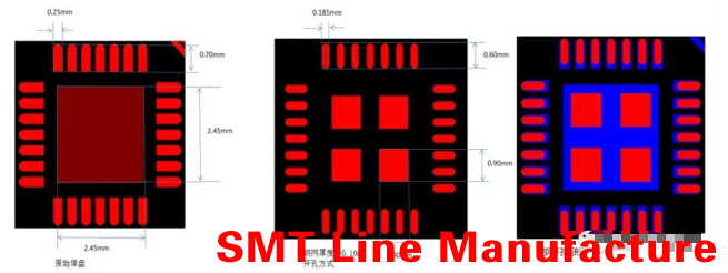
Poor pin coplanarity component steel mesh opening: surface mount common mode inductance component pins mostly use wire-wound structure, the pin coplanarity of this structure is very poor, the common mode inductance exceeds 0.2 mm; surface mount transformer components The number of pins is large, and the pin coplanarity is difficult to be consistent, exceeding 0.1 mm. Due to the poor coplanarity of these two components, the proportion of virtual soldering is relatively high. The package size of this type of device is generally large, and there is generally enough around the pad. Space, to solve the problem of virtual soldering, you can expand the stencil opening to increase the amount of solder paste, and use the aggregation effect of the solder paste to make up for the defect of poor coplanarity during soldering. It should be noted that the position of the enlarged opening must be avoided to contact the solder paste with the non-welded part of the component body, so as to avoid tin beading. The following are examples of solving common mode inductance and transformer false welding problems by expanding the stencil opening. (Common mode inductance corresponds to the thickness of the steel mesh T=0.12 mm, and the corresponding steel mesh thickness of the transformer T=0.10 mm).
3.3 Requirement of steel mesh reference point
The reference point of the stencil is opened in a 1:1 manner according to the size and shape provided by the substrate data. Generally, the black blind hole is not penetrated on the reverse side of the printing. The interior is filled with black material EPOXY, and the diagonal distance of the printed board is selected as far as possible. The far datum point is used as the datum point of the stencil design to improve the printing accuracy.
3.4 Steel mesh structure requirements
1) It has good flatness. The flatness of the screen frame is the most basic element of a qualified screen frame, which can be checked from the appearance. The conventional method is to place the screen frame flat on a flat glass table and observe the screen frame Whether it is in full contact with the table surface and there is no gap (the flatness tolerance of the screen frame is ±0.05 mm). The qualified screen frame can be completely touched.
2) Balanced tension on all four sides and good stress-strain ability. The frame tension is an important factor for a qualified steel mesh. The tension of the steel mesh is between 30N and 50N. The size of the tension is related to the size of the screen frame. The tension of the small screen frame is relatively lower between 30N and 40N, and the tension of the large screen frame is more than 55 CM×65 CM, and the tension is generally between 40N and 50N.
3) Printed graphics in the center.
4) The ratio of sufficient stencil area to printed graphics.
Assembly Line LED Lights,
LED Light Assemble Easy Line,
High Precision PCB Stencil Printer,
Full SMD Assembly Screen Stencil Printer,
Mini Reflow Oven,
SMT Lead-Free Wave Soldering Machine,
Hot Sale LED SMD SMT Pick And Place Machine,
HandLED Pick And Place,
SMT550 Pick And Place,
PCB Pick And Place,
Pick And Place Free Source,
Vacuum Pump For Pick And Place,
PCB Screening Conveyor SMT,
SMT Loader Suction,
SMT Loader Suction Machine,
SMT Monorail Track Conveyor,
Solder Robot High Quality Desktop Soldering Robot,
Multi-Axis Desktop Toy PCB Automatic Soldering Robot / Soldering Machine