
EMC and safety design of USB 3.0 interface circuit
From: Author: Publish time:2021-09-10 14:00 Clicks:0
EMC design and interface design are closely related, and the EMC indicators of many products are realized by reasonable interface circuit schemes. Through a detailed analysis of the EMC and safety design requirements of the USB 3.0 interface, a complete set of solutions for the EMC and safety design of the USB 3.0 interface is provided in terms of electrostatic protection, signal line EMI suppression, power supply current limiting, and voltage stabilization filtering. After testing and verification, the design completely meets the EMC and safety requirements of the USB interface such as CE certification.
USB (Universal Serial Bus) refers to "Universal Serial Bus". The USB interface is one of the most common universal external data interfaces, and has become a standard interface for all computing systems such as laptops, desktops, and servers.
With the rapid development of integrated circuits and people's demand for large-capacity data and high transmission rates, the new USB 3.0 interface has been widely used. The transmission rate of USB 3.0 is 5Gbps, which is 10 times that of USB 2.0. At the same time, the maximum power supply current is 1A, which puts forward higher requirements for the EMC and safety design of the line.
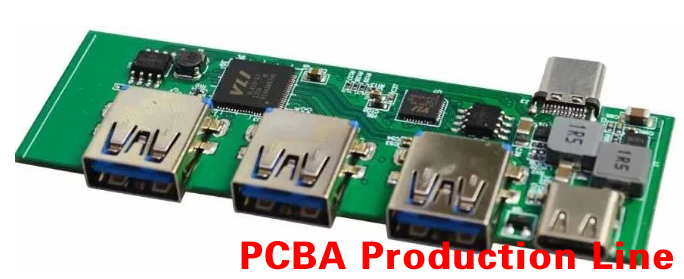
I.C.T is a manufacturer of SMT machines. It mainly provides customers with SMT production lines including SMT Stencil Printers, Pick and place machines, Reflow Oven, AOI Machine, Wave Soldering Machine and PCB Handling Machine etc. I.C.T has more than 25 researches on SMT and DIP technology, for the world Customers provide SMT total solutions. There are successful cases of SMT technICal team in Asia, Europe, AmerICa, AfrICa, and Australia.
More details, please contact us:
Tel: +86 13670124230 (WhatsApp/Skype/WeChat)
Email: etaSMT@foxmail.com
1 EMC and safety system solutions
The USB 3.0 interface adopts a high-speed differential signal transmission method. Due to the high-speed conversion of signal high and low levels during operation, the ground layer and power layer will generate a lot of high-frequency noise. Therefore, it is necessary to try to eliminate the common mode noise on the high-speed signal to ensure the signal Completeness.
Electrostatic discharge (ESD) may occur when users hot-plug USB peripherals, and air discharge may also occur within a few centimeters of the conductive surface, which may damage the USB interface and the chip. In addition, there is a 5V power supply in the USB interface, and the energy of the power supply must be effectively limited to prevent personal injury caused by power failure.
Therefore, the key to the design of the USB interface circuit is to improve the transmission quality of the USB signal, reduce electromagnetic interference, improve the ability to resist electrostatic interference, and ensure the safety of the power supply.
2 Scheme design
2.1 Electrostatic protection design
According to the electromagnetic compatibility directive 2014/30/EU followed by the international CE certification of products, the test requirements for the immunity of IT equipment to electrostatic discharge are contact discharge ±4kV, air discharge ±8kV; the test requirements for the immunity of communication products to electrostatic discharge are Contact discharge ±6kV, air discharge ±8kV. In addition, according to IEC61000-4-2:2008 "Testing and Testing Technology-Electrostatic Discharge Immunity Test", in addition to special requirements, the current highest requirements for electrostatic discharge test levels are contact discharge ±8kV and air discharge ±15kV.
Electrostatic discharge will cause transient overvoltage, which may appear on both the power bus and the data bus. Therefore, the USB interface protection circuit should include two parts: signal overvoltage protection and power supply Vbus overvoltage protection. For high-speed data signals, adding any capacitance to the data line may cause distortion of the signal waveform, leading to interruption and/or failure of data transmission. This puts forward higher requirements for the electrostatic discharge protection devices used on the USB 3.0 interface, which not only protects sensitive circuits, but also does not increase the capacitance that will reduce the signal quality.
At present, the most commonly used electrostatic discharge protection device is a protection module that combines a transient voltage absorption diode TVS and a clamping diode. The following recommends a USB 3.0 electrostatic discharge protection design. According to the characteristics of USB 3.0 to be compatible with USB 2.0, the electrostatic protection of USB 3.0 is divided into two parts: Vbus and a pair of differential lines compatible with USB 2.0 (D+ and D-) share one Four-pin TVS protection module (recommended to choose a protection device with a minimum reverse breakdown voltage of 6V and a junction capacitance of less than 1pF) for protection; two new pairs of differential lines SSTX+/- and SSRX+/- share a six-pin TVS protection module (It is recommended to choose a protection device with a minimum reverse breakdown voltage of 4V and a junction capacitance of less than 0.5pF) for protection.
On the premise of meeting the requirements of electrostatic discharge protection, the protective device can be reasonably selected according to the layout and wiring, cost and protection level, and it is not limited to the above recommended devices.
2.2 Signal line EMI suppression
On the basis of retaining the original pair of USB 2.0 differential signal lines, USB 3.0 adds two pairs of parallel high-speed differential signal lines to achieve high-speed transmission. The ultra-high transmission rate makes the signal line EMI radiation more serious, and at the same time it is easier to generate common mode noise, so the EMI of the interface must be suppressed.
Common mode choke inductors connected in series on the differential line can effectively suppress common mode noise. The common mode choke inductance of the USB 2.0 compatible data line in the USB 3.0 interface can use USB 2.0 devices, such as Sunlord's C2W2012FS900MST, or MURATA's DLW21SN900SQ2. The newly added two pairs of differential lines require common mode choke inductors to have a higher cut-off frequency and smaller insertion loss.
Common mode choke inductors are effective devices for suppressing common mode interference signals. There are many manufacturers and models available on the market. It can be selected reasonably according to the actual situation. The EMI suppression of Vbus is achieved through the power supply's voltage stabilization filter.
2.3 Power supply voltage regulator filter design
The USB power supply Vbus adopts LC filter mode or π-type filter, as shown in Figure 4. The maximum current provided by the USB 3.0 power system to each port is up to 1A, and the power supply voltage should be maintained in the range of 5 (1±0.05) V, that is, the interface power supply voltage is 4.75~5.25V, so the voltage drop from the USB power supply to the USB connector Generally, it cannot exceed 0.25V, and the voltage drop on the L1 magnetic bead (or inductance) generally does not exceed 0.1V. Considering the maximum supply current of 1A, the DC resistance of the magnetic bead should be less than 0.1Ω, and the rated current should be greater than 1A.
Considering the current capacity and volume of the current limiting circuit, the rated current of the magnetic beads is 5A, and the maximum DC impedance is 0.01Ω. The main function of the large capacitor C1 is the energy storage and stabilization of the power supply, with a capacitance value of 100μF and a rated voltage of 25V; the main function of the small capacitor C2 is filtering, with a capacitance value of 0.1μF and a rated voltage of 16V. Capacitors can choose ordinary electrolytic capacitors or ceramic capacitors, and the capacitance and number of capacitors can be flexibly adjusted according to the situation.
2.4 Power supply current limiting safety design
The Vbus in the USB interface is a restricted power source. According to IEC 60950:2007 "General Requirements for the Safety of Information Technology Equipment" or the latest IEC 62368:2014 "Safety Requirements for Audio and Video, Information and Communication Technology Equipment", the output of Vbus must meet the requirements of the standard The output current limit requirements. There are currently two main solutions for USB power supply current limiting design: stringing a positive temperature coefficient thermistor PTC on Vbus, or using a special current limiting switch chip.
When the circuit is working normally, the PTC temperature is close to room temperature, and the resistance is very small. It will not hinder the flow of current when connected in series in the circuit; and when the circuit has an overcurrent due to a fault, the PTC temperature rises above the switching temperature due to the increase in heating power. In a sudden increase, the current in the loop quickly decreases to a safe value, as shown in Figure 4.
The current-limiting switch chip is connected in series between the power supply and the load circuit. Due to the use of a power MOSFET with an on-resistance of milliohms as the switch, the loss introduced is extremely small. When the load circuit is overloaded or short-circuited, the current-limiting switch chip limits the current output to ensure the safety of the circuit. A current-limiting switch chip can provide current-limiting protection for one or more USB power sources.
PTC recommends selecting the maximum holding current of 2A, the smaller the DC impedance, the better (the DC impedance of PTC is generally about a few milliohms); there are multiple manufacturers and models of current limiting chips to choose from, and it is recommended to select a current limiting range of 1~5A. chip.
PTC current-limiting circuit is simple and low-cost, but the current-limiting is inaccurate, and is affected by ambient temperature; the current-limiting chip has more accurate current-limiting, quick action, and is not affected by ambient temperature, and one chip can provide multiple USB channels at the same time. Current limit protection, but the circuit is complicated and the cost is high.
3 EMC and safety program test
The EMC and safety design scheme of USB 3.0 in Figure 1 has been applied to many products, and the test and verification results have fully proved its effectiveness.
3.1 Electrostatic discharge test
The USB 3.0 interface has been subjected to electrostatic standard test verification under load and without load, as well as non-standard endurance test. In order to further verify the effectiveness of the protection scheme, the electrostatic withstand capability of the interface after removing the protection device was tested.
The test results show that the ESD protection scheme can meet the requirements of contact discharge ±8kV and air discharge ±15kV regardless of whether the USB 3.0 interface is loaded (such as mobile hard disk reading and writing) or without load (the interface does not plug in peripherals).
The electrostatic tolerance test of the signal line is to weld the eight wires of the USB 3.0 interface (six differential wires, one power supply Vbus and one GND) to the electrostatic test board through the cable, and use an electrostatic gun to test each signal in turn Conduct the contact discharge test on the wire, and the electrostatic test level is from low to high; after each signal wire is tested, observe whether the service function of the USB 3.0 port is normal. Only if the service function is normal, the test is judged to pass, otherwise it is not passed.
Figure 2 The electrostatic tolerance of the USB 3.0 interface under the protection scheme is up to 6kV. The USB 3.0 interface without any protection has the highest electrostatic tolerance of 1kV, and the USB is damaged when the electrostatic test is 1.5kV.
3.2 Interface radiation emission test
The radiation emission of four USB 3.0 ports is tested, the port is equipped with a mobile hard disk, and the mobile hard disk is read and written with the test tool. The details are as follows:
(1) USB 3.0 with USB 2.0 mobile hard disk
USB 3.0 is used for USB 2.0 peripherals, and the frequency point related to the radiation of the USB port is mainly 480MHz. The test results show that: only a pair of USB 2.0 compatible differential lines D+/- in USB 3.0 with common mode inductors can meet EN 300386:2008 "Electromagnetic Compatibility Requirements for Communication Equipment" or CISPR 22:2006 "Radio for Information Technology Equipment" The requirements of ClassA or ClassB in "Disturbance Limits and Measurement Methods". After adding a common mode inductor to D+/-, the radiation at 480MHz can be reduced by 6~10dB.
(2) USB 3.0 with USB 3.0 mobile hard disk
USB 3.0 is used for USB 3.0 peripherals, and the frequency point related to the radiation of the USB port is mainly 5GHz. The test results show that the common mode inductors are added to the three pairs of differential lines, and the 5GHz radiation is reduced by about 6dB, which meets the requirements of ClassA or ClassB.
(3) Spread spectrum technology
Under the premise of meeting the signal integrity, using the development frequency technology (more and more CPU and IC chips support the development frequency technology), the 5GHz radiation is significantly reduced, which can be reduced by about 10dB. If the system is running frequency, you can only add a common mode inductor to a pair of USB 2.0-compatible differential lines D+/- to suppress 480 MHz radiation. The two new pairs of differential lines can be omitted.
The electromagnetic radiation of the USB port is not only related to the design of the principle scheme of the port, but also closely related to the layout and wiring design of the PCB, structural design and cables. The EMI suppression scheme should be selected reasonably according to the product characteristics and application environment.
3.3 Interface current-limiting circuit test
It is recommended to select PTC maximum holding current 2A, minimum operating current 4A, operating time 1s@8A, DC impedance 8mΩ. The current-limiting chip uses a current-limiting range of 1.1 to 1.9 A, and a current-limiting response time of 0.6 ms. According to IEC 60950:2007 or IEC 62368:2014 for restricted power supply test requirements, the power supply PTC current-limiting scheme and current-limiting chip scheme in the USB 3.0 interface circuit were tested respectively. The test results show that both schemes meet the standard Require.
In order to compare the characteristics and differences between the current-limiting chip and the PTC current-limiting and the main factors that affect the start of the load, the load capacity of the two current-limiting schemes was tested. Connect an electronic load to the USB 3.0 interface, adjust the electronic load and observe the voltage and current changes of the USB 3.0 interface Vbus.
When the design exceeds 2 A to start the current limit, the test results show that: the PTC current limit scheme and the current limit chip start the current limit when the measured current reaches 5 A and 2.2 A respectively. It can be seen that the PTC current limiting is not accurate, and the current limiting chip is more accurate and quick to move, which only takes a few microseconds.
In short, both the current limiting chip and PTC can be used to limit the current of the USB 3.0 power supply, and both can meet the requirements of relevant safety standards. The test also found that the USB load terminal voltage is very affected by the quality of the peripheral cable (the impedance of the cable is very different). When using a large current to drive the peripheral, you should try to choose a short and thick (low impedance) cable to reduce The voltage drop on the cable ensures that the peripherals can work normally.
4 Conclusion
The EMC and safety design of the USB interface can be flexibly selected and modified for each part of the design according to actual use requirements to meet the principle of economical applicability.
For electrostatic protection, the three pairs of differential signal lines of the USB 3.0 interface and the power supply Vbus must be designed with electrostatic protection circuits.
For radiation suppression, the USB 3.0 interface is compatible with USB 2.0. A pair of differential lines add common mode choke inductors. For the newly added two pairs of differential lines, you can determine whether to add common mode choke inductors according to actual needs; if the port radiation only needs to meet Class A requirements, or if the system uses frequency technology, common mode choke inductance is not required; if the USB 3.0 interface is connected to a security device, such as an external camera, the USB extension cable is longer, common mode inductance should be added, and so on.
Vbus power current-limiting devices can be selected according to user needs. If users only use low-speed and low-power devices such as mice and keyboards, 1 A current-limiting devices should be selected; if users use high-speed and high-power devices, such as optical drives, mobile hard drives, or need to For other equipment to provide power, etc., choose a 2 A current-limiting device. Both PTC and current-limiting chips can be used as current-limiting devices. The former is accurate and fast, but expensive; the latter is affected by ambient temperature and slow in action, and the price is only one-tenth of the current-limiting chip.
LED Bulb Light Assemble Manual Line, SMT Screening Assembly Line, Solder Paste Printer, Online Solder Paste Printer, Vertical Reflow Oven, PCBA Automatic Selective Wave Soldering Machine, SMT Labeling Machine, SMT Soldering Machine, SMT Unloader Machine, Auto Splicing Machine SMT, SMT Automatic Splicing Machine, SMT Pick & Place Machine, AOI Automated Optical Inspection, Automated Optical Inspection Machine, Optical Inspection System, Solder Automatic Dispensing Robot Power Supply, Working 3 Axis Automatic Desktop Soldering Robot