
Various inspection standards for PCBA soldering appearance inspection!
From: Author:Mark Hardy Publish time:2021-09-10 14:24 Clicks:0
1. PCBA component design and inspection specifications
Inspection preparation The inspector must wear anti-static gloves and a watch, prepare calipers, electrical performance parameter instruments and other tools;
1. Technical requirements
1.1 PCBA component plates must be made of materials above 94-V0 flame retardant grade, and have corresponding UL yellow cards;
1.2 The appearance of PCBA component sheet has no rough burrs, poor cutting, delamination and cracking, etc.;
1.3 PCBA component plate size, aperture and margin meet the requirements of engineering drawings, and the unmarked tolerance value is ±0.1mm; unless required, the plate thickness is 1.6±0.1mm;
1.4 PCBA components must print production (design) date, UL symbol, certificate number, 94V-0 characters, factory logo, product model; if the PCBA component consists of multiple PCB boards, the rest of the PCB boards should also print the above content;
1.5 The printed character number and font size should be clear and discernible as the principle;
1.6 If the PCBA component adopts a resistance-capacitance step-down circuit, a half-wave rectifier circuit must be used to improve the safety and stability of the circuit;
1.7 If a switching power supply circuit is used for PCBA components, the standby power consumption must be less than 0.5W;
1.8 The standby power consumption of PCBA for European products must be less than 1W. If the US version PCBA customers have special requirements, the standby power consumption shall be implemented in accordance with the technical requirements;
1.9 The luminous tube uses all green or all red φ3 bright astigmatism except for the power lamp with φ5 amber high-brightness astigmatism; 1.10 PCBA components stipulate live wire (ACL), neutral wire (ACN), relay common terminal wire (ACL1), High-grade or continuous line (HI), low-grade line LO;
I.C.T is a manufacturer of SMT machines. It mainly provides customers with SMT production lines including SMT Stencil Printers, Pick and place machines, Reflow Oven, AOI Machine, Wave Soldering Machine and PCB Handling Machine etc. I.C.T has more than 25 researches on SMT and DIP technology, for the world Customers provide SMT total solutions. There are successful cases of SMT technICal team in Asia, Europe, AmerICa, AfrICa, and Australia.
More details, please contact us:
Tel: +86 13670124230 (WhatsApp/Skype/WeChat)
Email: etaSMT@foxmail.com
1.11 The welding fuse and CBB capacitor (resistance-capacitance circuit) of PCBA components must be on the live wire (ACL);
1.12 ACL1 must be connected to the live wire, HI or LO connected to each end of the heating element, and the common end of the heating element must be connected to the neutral line;
1.13 The solder joints of PCBA components must not have false soldering, continuous soldering, desoldering, and the soldering joints are smooth, uniform, free of bubbles, pinholes, etc.;
picture
2. Selection of components
2.1 PCBA component components are preferred to use well-known brand manufacturers, followed by manufacturers that meet international standards or industry standards; manufacturer components that do not use corporate standards;
2.2 Integrated block components (IC) use industrial-grade IC;
2.3 Connecting plug-ins and terminals must have UL certification and provide certificates;
2.4 The resistor components are made of metal film resistors with clear color rings, and the manufacturer complies with industry standards;
2.5 Electrolytic capacitor components use explosion-proof capacitors with a working temperature of -40—105℃, and the manufacturer meets industry standards;
2.6 Crystal components should be used for crystal oscillator components. RC or chip built-in is not recommended, and the manufacturer complies with international standards;
2.7 The diodes or transistors are selected from domestic well-known brands, which meet the industry standards;
2.8 The dump switch uses infrared photoelectric type instead of mechanical type;
2.9 The surface of the specified components must be printed with UL/VDE/CQC/symbols, trademarks, parameters, etc. and clearly visible;
2.10 The relevant wires must have UL/VDE symbols, wire gauges, certification numbers and manufacturer names, etc., and are clearly visible;
picture
3. Test and inspection
3.1 PCBA components are installed on the corresponding test tooling table, and the parameters such as voltage and frequency are adjusted;
3.2 Whether the PCBA component self-checking function meets the requirements of the functional specification, whether the relay output has abnormal noise, and whether the LEDs are all on evenly; 3.3 Whether the placement of the PCBA component dumping device and the output function during dumping comply with the functional specification;
3.4 When the temperature probe of the PCBA component is disconnected or short-circuited, whether the output function and fault indication comply with the functional specification;
3.5 Whether the function output of each button of the PCBA component meets the requirements of the function specification;
3.6 The ambient temperature of PCBA components indicates whether the temperature displayed by the LED or digital tube complies with the functional specification;
3.7 The power status of the PCBA component indicates whether the LED complies with the functional specification;
3.8 Whether the intelligent control operation mode of PCBA components meets the functional specifications;
3.9 Whether the continuous operation mode of PCBA components meets the functional specifications;
3.10 Whether the standby power consumption of PCBA components meets the functional specifications;
3.11 The voltage is adjusted to 80% of the rated voltage, whether the relay output has abnormal noise, and whether the LED brightness is uniform;
3.12 The voltage is adjusted to 1.24 times of the rated voltage, whether there is any abnormal noise in the relay output, and whether the LED brightness is uniform;
picture
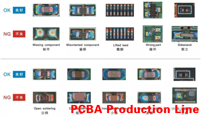
2. PCBA general appearance inspection specification
1. Solder joint: The wetting angle between the fillet weld with poor contact angle and the end joint of the land pattern is greater than 90°.
2. Upright: One end of the component leaves the pad and rises diagonally or upright.
3. Short circuit: the solder between two or more solder joints that should not be connected is connected, or the solder of the solder joint is connected with an adjacent wire.
4. Empty soldering: that is, the component leads and the PCB solder joints are not connected by soldering.
5. Fake soldering: The component leads and the PCB solder joints seem to be connected, but they are not actually connected.
6. Cold soldering: The solder paste at the solder joints is not completely melted or metal alloys are not formed.
7. Less tin (not enough tin): The area or height of the component end and the PAD does not meet the requirements.
8. Too much tin (too much tin): The area or height of the component end and the PAD who eat tin exceeds the requirement.
9. The solder joints are black: the solder joints are black and dull.
10. Oxidation: The surface of components, circuits, PAD or solder joints has produced chemical reactions and colored oxides.
11. Displacement: The component deviates from a predetermined position in the horizontal (horizontal), vertical (vertical) or rotational direction in the plane of the pad (based on the centerline of the component and the centerline of the pad).
12. Polarity reversal (reverse): the direction of the component with polarity or the polarity that does not meet the requirements of the document (BOM, ECN, component location diagram, etc.) is reversed.
13. Floating height: There is a gap or height between the components and the PCB.
14. Wrong parts: component specifications, models, parameters, shape and other requirements are not consistent with (BOM, samples, customer information, etc.).
15. Tin tip: The solder joints of the components are not smooth, and the tip is pulled.
16. Multiple pieces: According to BOM and ECN or sample board, etc., there are multiple pieces where parts should not be installed or redundant parts on the PCB.
17. Missing parts: According to BOM and ECN or prototypes, etc., the parts should be installed on the position or on the PCB, but the parts are missing.
18. Dislocation: The position of the component or component pin is moved to the position of other PAD or pin.
19. Open circuit (open circuit): PCB circuit disconnection phenomenon.
20. Side placement (side stand): chip components with different width and height are placed on the side.
21. Inverted white (turned side): Two symmetrical surfaces with different components interchange positions (such as: the side with silk-screen logo and the side without silk-screen logo are upside down), chip resistors are common.
22. Tin beads: small tin spots between the feet of components or outside of the PAD.
23. Air bubbles: There are air bubbles inside solder joints, components or PCB.
24. Tin on (climbing tin): The height of the solder joints of the components exceeds the required height.
25. Tin crack: The solder joint is cracked.
26. Hole plug: PCB plug-in hole or via hole is blocked by solder or other.
27. Damage: cracks or cuts or damages in components, board bottom, board surface, copper foil, circuit, through hole, etc.
28. Blurred silk screen: The text or silk screen of the components or PCB is blurred or broken, and cannot be recognized or blurred.
29. Dirty: The board surface is not clean, there are foreign objects or stains and other defects.
30. Scratches: PCB or buttons are scratched and copper foil is exposed.
31. Deformation: Components or PCB body or corners are not on the same plane or bent.
32. Blistering (layered) PCB or components are layered with copper and platinum, and there is a gap.
33. Overflowing glue (too much glue) (too much red glue) or overflowing the required range.
34. Less glue (too little amount of red glue) or not up to the required range.
35. Pinhole (concave): PCB, PAD, solder joints, etc. have pinhole concavities.
36. Burr (over the peak): PCB board edge or burr exceeds the required range or length.
37. Gold finger impurities: There are pitting, tin spots or solder mask on the surface of the gold finger coating.
38. Gold finger scratches: There are scratches or bare copper and platinum on the surface of the gold finger plating.
SMT Line Visual Lighting LED Display, Assembly Line TV, Semi Automatic SMT Stencil Printer, , Reflow Oven Thermocouple, Mini Double Wave Soldering Machine, Mobile SMT Machine, Pick And Place Desktop, SMT Pick And Place 500MM, Sticker Placement Machine For Injection, SMT Assembly Machine, SMT Splicing Machine, AOI Inspection Systems, SPI SMT Machine, AOI Machine For PCB, 3D Automated Optical Inspection, Automated Optical Inspection Companies, Automatic Screw Fixing Robot, Automatic Screw Fastening Robot, Screws For Robot Car, Screw Tightening Robot Janome, Electric Screw Driving Robot